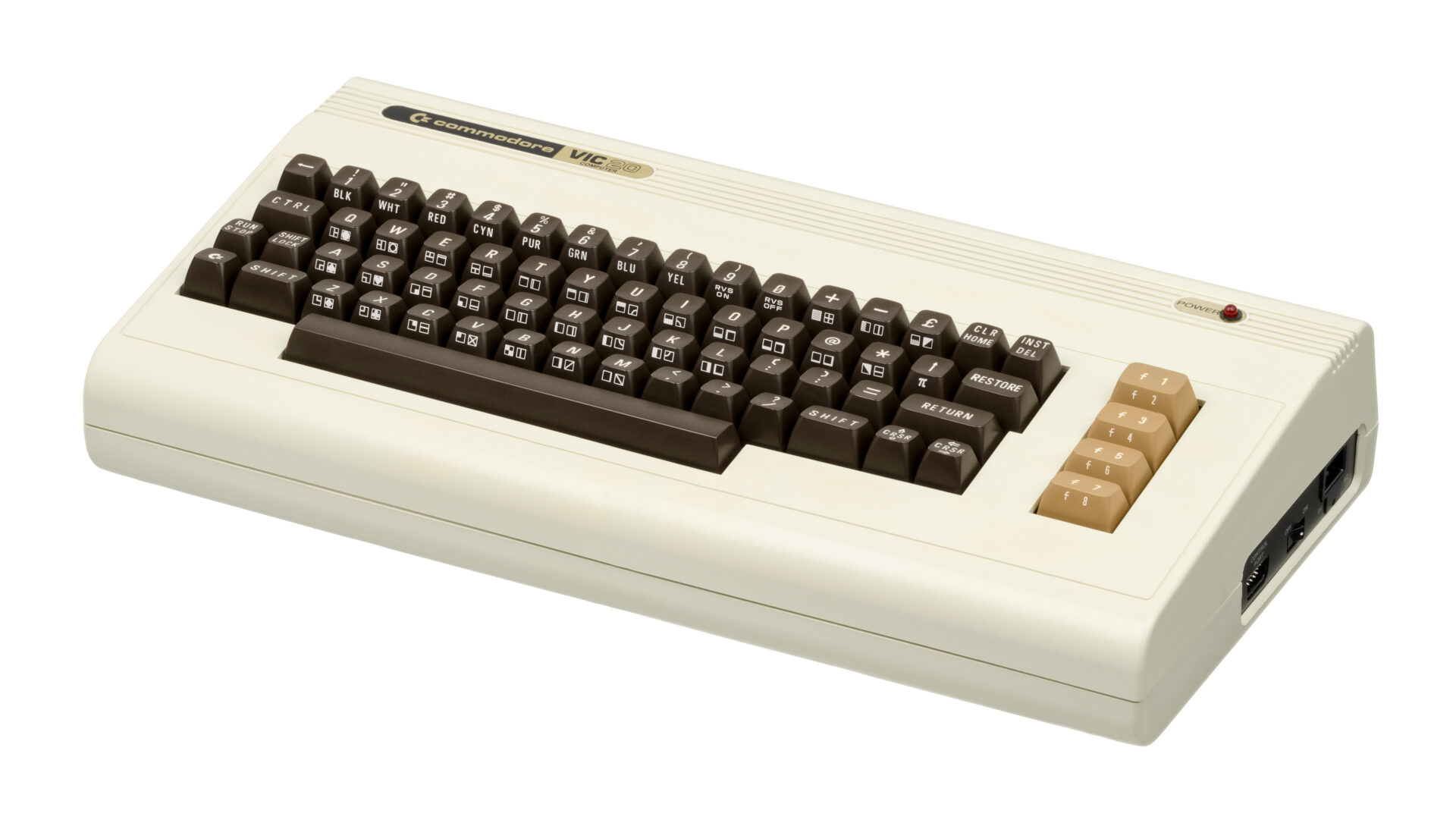
Especificaciones Técnicas
| Especificaciones Técnicas | |||
|---|---|---|---|
| Nombre | |||
| Fabricante | |||
| Nombres Alt. | |||
| Origen | |||
| Año | 1982 | ||
| Lenguaje integrado | |||
| Teclado | |||
| CPU | MOS 6502 @ 1.10 MHz | ||
| Video | |||
| Audio | |||
| RAM | |||
| ROM | |||
| Modos de Texto | |||
| Modos Gráficos | |||
| Sonido | |||
| Puertos de E/S | |||
| Alimentación | |||
| Periféricos | |||
Los conectores del VIC-20 son los siguientes.
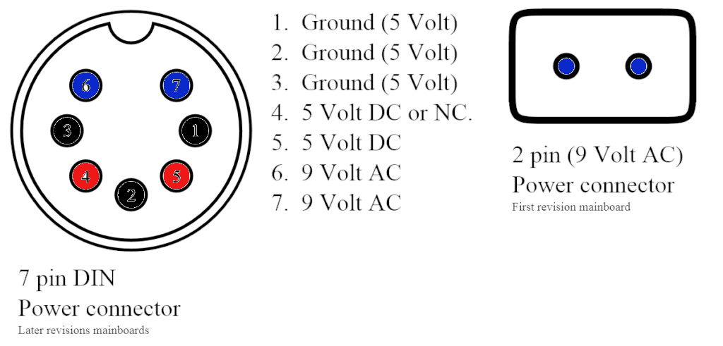
| Alimentación |
El conector de alimentación es, salvo en los primeros modelos, un DIN 7 :
| Video |
La salida de vídeo del VIC-20 es un conector DIN 5 (DIN41524) Hembra.

| Pin | Name | Dir | Description |
|---|---|---|---|
| 1 | +6V | OUT | +6 VDC (10 mA max) |
| 2 | GND | – | Ground |
| 3 | AUDIO | OUT | Audio |
| 4 | VLOW | OUT | Video Low |
| 5 | VHIGH | OUT | Video High |
El VIC-20 tiene dos señales de video en su conector:
- Video Low (VLOW): esta señal tiene un filtro de paso bajo aplicado, lo que reduce los componentes de alta frecuencia y puede dar como resultado una imagen más suave y borrosa.
- Video High (VHIGH): esta señal VHIGH no se filtra, conservando su contenido original de alta frecuencia. Esto significa que VHIGH puede producir una imagen más nítida y detallada, pero también más propensa al ruido y los artefactos.
Hay diferencias dependiendo de la revisión de VIC-20. Así, algunas revisiones, como las versiones de costo reducido, pueden no incluir el filtro de paso bajo en la ruta de la señal VLOW, lo que hace que ambas salidas sean similares. Esta variación en el diseño puede dar como resultado una calidad de video diferente entre máquinas individuales.
Mejorar la salida de video compuesto del VIC-20:
- Sacar el 6561 del socket.
- Doblar el PIN #2 hacia fuera.
- Insertar el 6561 en el socket.
- Conectar al pin doblado un condensador cerámico 104 (100nF) y una resistencia de 360R. Esta línea es ahora únicamente LUMA (Luminancia).
- La salida en el socket es CHROMA (Crominancia).
| Cassette |
| PIN # | Tipo |
|---|---|
| A-1 | GND |
| B-2 | +5V DC |
| C-3 | MOTOR (Motor Control, approximately 6 Volt power supply for the motor) |
| D-4 | READ (Data Input, read data from datasette) |
| E-5 | WRITE (Data Output, write data to datasette) |
| F-6 | SENSE (Detection, if one of the keys PLAY, RECORD, F.FWD or REW is pressed) |
| Serial / Disk Drive |
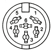
El puerto serie es un conector DIN de 6 pines (DIN 45322). Utilizado para conectar unidades de discos o impresoras, es una variación del bus paralelo IEEE-488/IEC-625.
En teoría pueden conectarse hasta 31 dispositivos encadenados, ya que se reservan 32 números de dispositivos (del 0 al 31) y el dispositivo 31 está reservado (UNTALK/UNLISTEN). En la realidad son menos, ya que por un lado, los números de dispositivos del 0 al 4 se usan internamente (ej: el 1 es el Datasette). Y por otro lado, el límite es físico dado por la corriente que el chip controlador puede consumir. El límite real suele ser de 8 dispositivos.
| Pin | Tipo | Comentario |
| 1 | SERIAL SRQ IN | Serial service request in: Any device on the serial bus can bring this signal low when it requires attention from the VIC. The VIC will then take care of the device. |
| 2 | GND | Ground |
| 3 | SERIAL ATN IN/OUT | Serial attention in/out: The VIC uses this signal to start a command sequence for a device on the serial bus. When the VIC brings this signal low, all other devices on the bus start listening for the VIC to transmit an address. The device addressed must respond in a preset period of time; otherwise the VIC will assume that the device addressed is not on the bus, and will return an error in the status word. |
| 4 | SERIAL CLK IN/OUT | Serial clock in/out: This signal is used for timing on the serial bus. |
| 5 | SERIAL DATA IN/OUT | Serial data in/out: Data on the serial bus is transmitted one bit at a time on this line. |
| 6 | NO CONNECTION | Note: in some models pin 6 is /RESET |
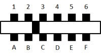
| Puerto del usuario |
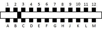
| Upper side | ||
| 1 | GND | Ground |
| 2 | +5VDC | 100mA max |
| 3 | /RESET | By grounding this pin, the VIC will do a cold start, resetting completely and erasing any program in memory. |
| 4 | JOY0 | This pin is connected to joystick switch 0. |
| 5 | JOY1 | |
| 6 | JOY2 | |
| 7 | LIGHT PEN | This pin also acts ad the input for the joystick fire button. |
| 8 | CASSETTE SWITCH | This pin is connected to the sense cassette switch line. |
| 9 | SERIAL ATN IN | This pin is connected to the ATN IN line of the serial bus. |
| 10 | 9VAC | (+ phase) Connected directly to the VIC transformer. |
| 11 | 9VAC | (- phase) Connected directly to the VIC transformer. |
| 12 | GND | Ground |
| Bottom side | ||
| A | GND | Ground |
| B | CB1 | The VIC gives you complete control over Port B on VIA chip #1. Eight lines for input or output are available, as well as 2 lines for handshaking with an outside device. The I/O lines for Port B are controlled by two locations. One is the port itself, and is located at 37136 ($9110 hex). Naturally you PEEK it to read an input, or POKE it to set an output. Each of the eight I/O lines can be set up as either an input or an output by setting the data direction register properly. It is located at 37138 ($9112 hex). |
| C | PB0 | |
| D | PB1 | |
| E | PB2 | |
| F | PB3 | |
| G | PB4 | |
| H | PB5 | |
| J | PB6 | |
| K | PB7 | |
| L | CB2 | |
| M | GND | Ground |
| Puerto de expansión |
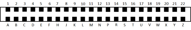
| Pin | Signal | Description | Comment |
|---|---|---|---|
| 1 | GND | Ground | (0 Volt) |
| 2 | D0 | data line 0 | data bus of the computer |
| 3 | D1 | data line 1 | |
| 4 | D2 | data line 2 | |
| 5 | D3 | data line 3 | |
| 6 | D4 | data line 4 | |
| 7 | D5 | data line 5 | |
| 8 | D6 | data line 6 | |
| 9 | D7 | data line 7 | |
| 10 | /BLK 1 | Memory block 1 | Chip select for block 1; active-low, if address on bus is within $2000-$3FFF. |
| 11 | /BLK 2 | Memory block 2 | Chip select for block 2; active-low, if address on bus is within $4000-$5FFF. |
| 12 | /BLK 3 | Memory block 3 | Chip select for block 3; active-low, if address on bus is within $6000-$7FFF. |
| 13 | /BLK 5 | Memory block 5 | Chip select for block 5; active-low, if address on bus is within $A000-$BFFF. |
| 14 | /RAM 1 | RAM 1 | Chip select for RAM (memory area $0400 – $07FF) |
| 15 | /RAM 2 | RAM 2 | Chip select for RAM (memory area $0800 – $0BFF) |
| 16 | /RAM 3 | RAM 3 | Chip select for RAM (memory area $0C00 – $0FFF) |
| 17 | V R/W | VIC Read – /Write | high during read cycle, low during write cycle of the VIC |
| 18 | C R/W | CPU Read – /Write | high during read cycle, low during write cycle of the CPU |
| 19 | /IRQ | Interrupt Request | Interrupt Request Line |
| 20 | NC | not connected | |
| 21 | +5V DC | Supply Voltage +5V DC | + 5 Volt DC. |
| 22 | GND | Ground | (0 Volt) |
| A | GND | Ground | (0 Volt) |
| B | A0 | address line 0 | address bus of the computer |
| C | A1 | address line 1 | |
| D | A2 | address line 2 | |
| E | A3 | address line 3 | |
| F | A4 | address line 4 | |
| H | A5 | address line 5 | |
| J | A6 | address line 6 | |
| K | A7 | address line 7 | |
| L | A8 | address line 8 | |
| M | A9 | address line 9 | |
| N | A10 | address line 10 | |
| P | A11 | address line 11 | |
| R | A12 | address line 12 | |
| S | A13 | address line 13 | |
| T | /I/O2 | input/output 2 | input/output area 2 ; active low, if address on the bus is within $9800-$9BFF. |
| U | /I/O3 | input/output 3 | input/output area 3 ; active low, if address on the bus is within $9C00-$9FFF. |
| V | SØ2 | S Phi 2 | system clock (1,108MHz for PAL, 1,018MHz for NTSC) |
| W | /NMI | non maskable interrupt | Non Maskable Interrupt Line |
| X | /RESET | Reset | If you pull this line to low, all chips will be re-initialized. The program counter of the CPU will be loaded with the reset-vector $FFFC and $FFFD (usually $FD22). |
| Y | NC | not connected | |
| Z | GND | Ground | (0 Volt) |
Tengo 4 VIC-20. Uno de ellos es una versión USA, nuevo en caja.
Todos llevan la misma revisión de placa. Sin embargo el acabado, número de chips en zócalo, y calidad de la terminación varía de unas a otra. La placa del VIC [2] tiene un peor acabado y la silk screen está “arrugada”.
También varían en el número de chips que llevan zócalo. Así la [1] lleva 7 chips en zócalo, la [0] y la [3] solo 4 chips lo llevan, y la [2] solo 2.
| Chip | [0] | [1] | [2] | [3] |
| MOS 6522 VIA (1) | X | |||
| MOS 6522 VIA (2) | X | X | X | |
| MOS 6561-101 (VIC) | X | X | X | X |
| MOS 901460-03 (Character ROM) | X | |||
| MOS 901486-01 (BASIC ROM) | X | |||
| MOS 901486-07 (KERNAL ROM) | X | X | X | X |
| MOS 6502 | X | X | X |
Todos los VIC-20 que tengo (incluyendo uno nuevo en caja) fallan , y a todos les pasa lo mismo: el LED de encendido se enciende pero no hay salida de video. En la web COMMODORE VIC20 COMPUTER – DIAGNOSTICS AND REPAIR he encontrado los posibles problemas que pueden ocurrir en esta versión de placa.
| LATEST VERSION CR BOARD: ASSY #250403 FAB #251040-01 REV D 1981/2 | ||||
|---|---|---|---|---|
| (note this model uses the same power pack as a C64) | ||||
| UAB1 | 6522 | VIA | INTERFACE, KEYBOARD-SERIAL | Startup screen normal, but no cursor. Keyboard doesn’t work at all. Partial failure: some keys “stuck” or don’t work… may be a whole row or column. Also may cause serial port (drive access) problems. Can produce blank screen if shorted (remove to check). |
| UAB3 | 6522 | VIA | INTERFACE, JOY-USER-SERIAL-CASS | Startup screen normal, but drive access problems (“SEARCHING FOR… ” forever). One or more joystick positions don’t work. No cassette or user port access. Can produce blank screen if shorted (remove to check). |
| UB4 | 7406 | LOGIC | Blank screen or serial port (disk drive) access problems. | |
| UB6 | LM555 | TIMER | POWER ON RESET | Will not reset on power up. May produce garbled or random screen characters-graphics, or screen may start up “frozen”. If drive resets when computer is powered up, this chip is OK. |
| UB7 | 6560-101 | VIC | VIDEO/AUDIO | White or blank screen, garbled or no video, screen full of (or few random) “garbage” characters. “Blind” disk commands may still work. Partial failure: Dark or smeary image, loss of color, garbled or no sound, game paddles or light pen doesn’t work. |
| UB9 | 7402 (M53202P) | OSC | MASTER CLOCK OSC | White screen… no RF interference in AM radio (see text). Partial failure: can produce missing color or incorrect colors, slight or severe tearing of picture or diagonal lines, sounds play at incorrect pitch. Symptoms may only appear after warmup. |
| UC2 | 74LS04 | LOGIC | Screen character colors incorrect (scrambled). If very bad, entire screen becomes garbled with flashing characters, vertical bars and random colors. | |
| UC3 | 74LS02 | LOGIC | ||
| UC4 | 74LS138 | LOGIC | MEMORY CONTROl | Blank screen. |
| UC5 | 74LS138 | LOGIC | BLOCK CONTROL | Blank screen. |
| UC6 | 74LS138 | LOGIC | I/O | |
| U14-U15 | MB8416A | RAM | MEMORY | Blank screen. Less than normal “3583 BYTES FREE” at startup. Sometimes will produce “garbage” screen or screen freeze after warmup. Shorted chips can get very hot. |
| UD1 | CD4066 | QUAD SWITCH | (LOGIC GATES) | Incorrect color on screen characters. |
| UD2 | 2114 | SRAM | ||
| UD7 | 901460-03 | ROM | CHARACTER | Startup screen characters missing (just blocks or flashing lines where characters should be) and alphanumerics missing from games. Game carts that use mostly graphics characters may look normal while running. |
| UD8 & UE8 | MPS65245 or MOS65245 or 74LS245 | TRI-STATE | LOGIC | Blank screen. Partial failure: garbled video or audio. see UB7 |
| UD9 | 74LS133 | LOGIC | ||
| UE1 | 2114 | SRAM | ||
| UE2 | 2114 | SRAM | ||
| UE10 | 6502 | MICROPROCESSOR | Blank screen. Partial failure: programs may run for awhile, then freeze. | |
| UE11 | 901486-01 | ROM | BASIC | Startup screen with borders but no characters. Disk commands do not work, but game carts still work. |
| UE12 | 901486-06 | ROM | KERNAL | Blank screen on startup, no drive access, game carts don’t work. Partial failure: some game carts may still work. This IC is a very common failure! |
| UF8 | MPS65245 or MOS65245 or 74LS245 | TRI-STATE | LOGIC | |
| U13 | 74LS08 | White garbled screen or blank screen. | ||
| Q3 | 2SD880 | TRANSISTOR, CASS. MOTOR DRIVER | Cassette motor doesn’t run. Common failure. | |
| CR2 | S10B | BRIDGE RECT, 1A, 50V | ||
| F1 | 1 AMP F8 | FUSE, 9 VOLT AC SOURCE | Opening screen normal and all functions work except cassette motor and 9VAC source to user port. | |
| Y1 | CRYSTAL, 14.31818MHz | See UB9 (master oscillator chip). | ||
Primero compruebo el procesador 6502. Para ello:
Hay que medir la tensión entre el polo negativo de C39 y el pin 40 del 6502 mientras se enciende el VIC-20. Inicialmente debe leerse una tensión por debajo de 2V (LOW) por algo más de un segundo y luego debe cambiar a 5V (HIGH). Si esto no ocurre, entonces seguramente está fallando el 555. Si es correcto hay que comprobar los pines siguientes:
- pin 1 = GND
- pin 2 = 5V (1 lógico)
- pin 3 = 2-3 V (Cambiando entre el 0 y el 1 lógicos rápidamente)
- pin 4 = 2-3 V
- pin 8 = 5 V
- pins 9 a 20 = 2-3 V
- pin 21 = GND
- pins 22 a 34 = 2-3 V
- pin 37 = 2-3 V
- pin 39 = 2-3 V
Luego he quitado todos los chips que vienen en zócalo en las tres placas (MOS 6522 VIA y MOS 901486-07 ROM KERNAL), y he probado combinaciones con ellos en la placa [1] que es la que tiene más zócalos.
Así he comprobado que está fallando un chip con la ROM KERNAL y seguramente uno de los VIA, ya que el VIC puede encender si falla el segundo VIA (2). Al final han quedado 2 placas funcionando. La otra la utilizaré para repuestos.
COLECCIÓN
| – 1 – |
| S/N | P1542256 | ||
| MB S/N | RS 00256655 | ||
| ASSY NO. | |||
| FAB NO. | |||
| FUNCIONA | NO?? | ||
| Comentario | Nuevo en caja. Versión USA. La fuente es de 117V, 1.0A y 60Hz. | ||
| – 2 – |
| S/N | WG-C-233176 | ||
| MB S/N | RS 00176865 | ||
| ASSY NO. | 250403 | ||
| FAB NO. | 251040-01 | ||
| FUNCIONA | SI | ||
| – 3 – |
| S/N | WG-C-223577 | ||
| MB S/N | UA 179787 | ||
| ASSY NO. | 250403 | ||
| FAB NO. | 251040-01 REV. D W-1894HB | ||
| FUNCIONA | NO | ||
| – 4 – |
| S/N | WG-B-182000 | ||
| MB S/N | 087293 | ||
| ASSY NO. | 250403 | ||
| FAB NO. | 251040-01 REV. D W-1894HB | ||
| FUNCIONA | SI | ||
| Comentario | En perfecto estado. Obtenido con un cartucho VIC-1110: 8K RAM Software | ||
| – 5 – |
| S/N | WG-B-181903 | ||
| FUNCIONA | NO | ||
SOFTWARE
| CARTUCHOS |
| VIC NO. | Nombre |
|---|---|
| 1914 | Adventure Land |
| 1931 | Clowns |
| 1912 | Mole Attack / Mole Hitting |
| 1925 | Money Wars |
| 1929 | Personal Finance |
| 1915 | Pirates Cove |
| 1913 | Raid on Fort Knox / Bank Robber / Raiders |
| 1933 | Speed Math & Bingo Math |
| 1902 | Star Battle / Galaxian |
| 1911 | The Sky is Falling / Sky Hole |
| 1938 | Tooth Invaders |
| 1901 | Avenger / VIC Avenger |
| DISKETTES |
| Nombre | Contenido | ||
|---|---|---|---|
| model 1551/1541 | test / demo-diskette single sided / 48 tpi | ||
Directorio:
Side 1:

13  HOW TO USE        PRG (engl. instruction 1.part)
5   HOW TO USE TWO    PRG (engl. instruction 2.part)
1   C-64 WEDGE        PRG (Utility Starter C64)
4   VIC-20 WEDGE      PRG (Utility Starter for VIC-20)
4   DOS 5.1           PRG (Utility Main Program)
11  COPY/ALL          PRG (Copy Program)
9   PRINTER TEST      PRG (Printer Test)
4   DISK ADDR CHANGE  PRG (Change device number by software)
4   DIR               PRG (Easier using of disk commands)
6   VIEW BAM          PRG (BAM Viewer)
4   CHECK DISK        PRG (Diskcheck with VALIDATE)
14  DISPLAY T&S       PRG (Block Viewer in Decimal or Hexadecimal)
9   PERFORMANCE TEST  PRG (Floppy Check)
5   SEQUENTIAL FILE   PRG (Program example for SEQ-files)
13  RANDOM FILE       PRG (Program example for special DOS-Commands)
558 BLOCKS FREE
El contenido del disco de demo/test puede cambiar dependiendo del año o del modelo.